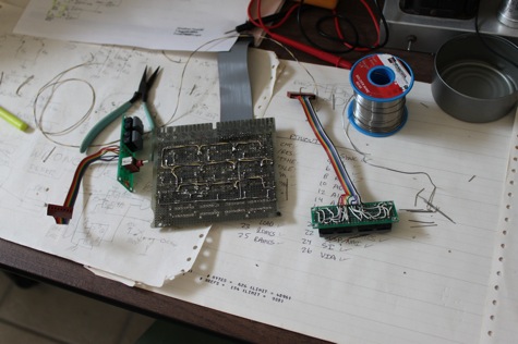
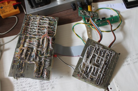
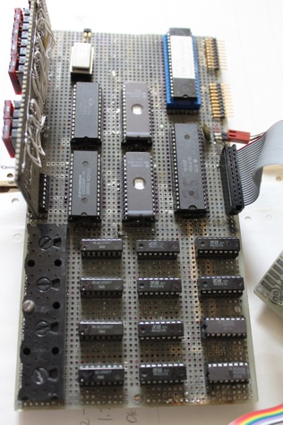
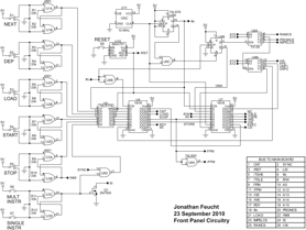
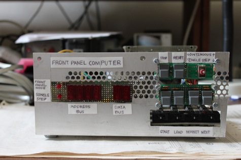
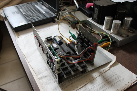
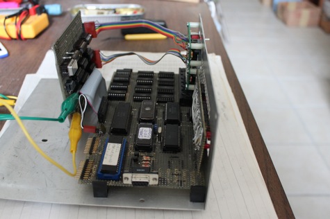
The circuitry consists of four sections: a main board, including the processor, thumb switches, and ACIA; the front panel logic board, consisting of several discreet logic chips; push buttons, for which the signals fed directly into the front panel logic board; and the display board, which consisted of a bunch of LED's which displayed the bits of the address and data busses on the main board. The wires from the push buttons fed directly into the front panel circuitry. My initial instructions were to simply get his system to work again. Although, early on, I knew it would be a bit more complicated than that, since the prototype board I was given had several disconnected wires, and I found out pretty quickly that the circuit did not match the schematic, and there were a few extra gates. I ended up reverting to the schematic, because I simply had no idea what the extra gates were used for, since some of the wires had become disconnected from the board. Also, the prototype design did not have any program or data memory chips, and did not yet have an ACIA. The project quickly turned into me redesigning the entire thing so it included memory.
In the process of revising the circuitry, I essentially had to learn how to solder. After completely reverting to the original design and including memory circuitry on the board after many hours of soldering and before I even began to start testing it, I found out that the circuitry of design did not meet the specifications my uncle wanted for the system, and the project quickly turned into a design problem. I quickly found that I did not possibly have enough room on the board to include all the chips I needed in order to make necessary improvements.
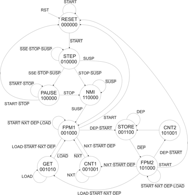
A much needed improvement was to replace many of the discreet logic chips with programmable logic devices (PLD's). The discrete logic chips contain four 2-input gates or two flip-flops in a 14-pin package, but with the GAL16V8, you have access to 8 flip-flops and hundreds of gates in a 20-pin package, so you could fit a lot more circuitry in a smaller area. They probably didn't even exist when my uncle designed the project back in 1976. I still used 2-input NOR gates to debounce the pushbuttons and a hex flop to synchronize the signals, but the rest of the circuitry is programmed onto the PLD's. With the PLD's, at least I could change the circuitry without having to unsolder and solder wires. I got my uncle's Superpro/Z programmer working for the first time, and began programming chips.
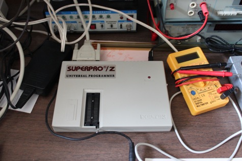
Left: The GAL programmer.
Right: A state machine diagram for the front panel switch logic, implemented on one GAL chip.
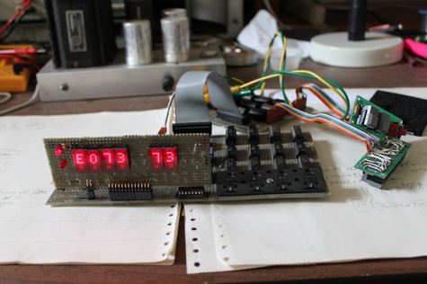
Another improvement with the system was the addition of header pins and connectors, so I could more easily connect and disconnect boards from each other. Also, I added new switches and buttons since the old buttons were rusty and difficult to press. And finally, I replaced all the LED's on the display board with six ancient TIL311 hexadecimal displays, four for the address bus, and two for the data bus. The display panel also included a couple status indicator LED's for status indication.
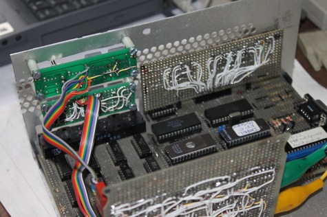
The wires left are +5 volt supply (yellow / purple wires) and ground (metal wires), with nothing else connected yet. The push buttons and one toggle switch are also included in the photos, and show the pin connectors used to connect the buttons to the front panel logic board.
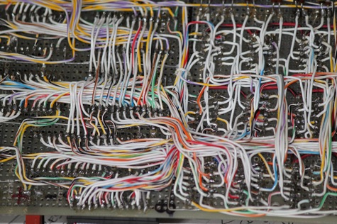
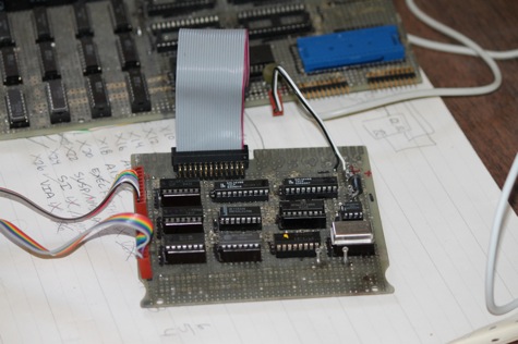
Left: Bottom view of main board
Right: Top view of front panel logic board, showing the two programmable logic devices
Debugging the circuitry took a couple days to do. I had a couple shorts with wires I needed to hunt down. I also added circuitry for RS-232 communication using TTL levels. I also began writing assembly programs to test out various systems on the board, translated them to 6502 machine code, then programmed them into the memory using the thumbwheels and the control switches. I then began using the EconoROM EPROM (erasable program memory) emulator working, so I could test programs on the system by downloading binaries from the computer.
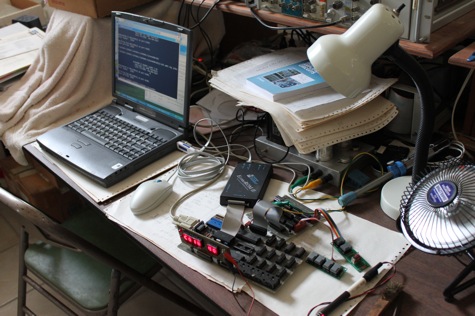
Left: In this picture, the development system is set up for terminal emulation via RS-232 cable, and the EPROM emulator is connected to the board.
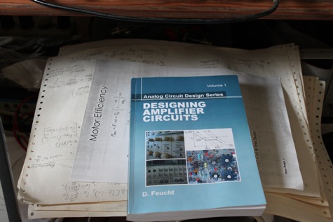
Right: A huge mound of papers with Uncle Dennis's Analog Amplifier Design book sitting on top.
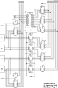
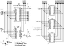
The main board, including processor, SRAM, EPROMS, VIA, ACIA, counters, bus arbitration circuitry, and TTL RS-232 circuitry


Left: The front panel computer running a test program off of the EPROM emulator.
Right: Uncle Dennis's amplifier design book, and a huge stack of papers I generated working through his book.
Finally, I cut up the the original aluminum case designed for the project and made a tacky stand for the front-panel computer out of scrap aluminum.
Lately, I've been working on trying to implement one of Uncle Dennis's thermal energy meters for use as an engine monitor for a generator. It's involving me learning a bit about Forth programming language, which Uncle Dennis uses for embedded computing applications. Compared to C, Forth is stack based, meaning there are no local variables in procedures. To call a subroutine, you push the arguments for the subroutine on the stack, then call the word, and the results of the subroutine will appear on the top of the stack. Also, Forth is also an interpreter. In C, you need to compile code before it will execute. In Forth, you're provided an interactive shell in which you could type in code and see what it does. Visual Basic supplies something similar with the debug window.
There are some things that make Forth an ideal language for many embedded computing applications, although it has a reputation as a 'write-only language', since Forth code is usually never formatted in a form where you can easily tell what it is doing by looking at it. For instance, a chunk of code from the Thermal Energy Meter looks something like this, no comments:
: FN FUNCTION @ 2* DUP 2* + FUNCTIONS + 6 0
 	DO DUP I + C@ DS I + C! LOOP DROP DS_TO_DIGITS ;
In his code, we have a subroutine named FN he didn't include many necessary comments. It is quite difficult to structure the code so that it's more readable. So to figure out what the code does, I had to manually go through each word and write out what is happening to the stack, and try to make sense out of it by converting it to C. The same code above converted to C would look something like this:
void FN() {
	for (int I = 0; I < 6; I++) {
		DS[I] = FUNCTIONS[FUNCTION * 6 + I];
	}
 	DS_TO_DIGITS();
}
Some people are convinced that Forth is the best programming language in the world. Although, after spending days trying to read the poorly-commented code for the Thermal Energy Meter, I'm kind of glad that it never caught on. Not only is Forth very cryptic, there are many nuances about the language that make programming and debugging much more complicated and time-consuming. If I had my way, I would never write another program in Forth ever again.
